1. How a transistor works
2. Some details about the manufacture
1. How a transistor works
Look at following details:
(A free electron encountering a hole will fill it, what makes both disapear: the free electron becomes a catched electron, part of the link between two silicon atoms, thus a constitutive part of the cristalic structure of the silicon.) (A hole is a lack of link between two atoms: one of the two atoms has an electron available to build a link, yet therefore two electrons are needed, so there is no link. Holes can move: if the link of one of the two atoms with one of his neighbours is broken, that will make one electron be available to build the missing link. Yet now there is another missing link just near. The hole has moved one atom.)
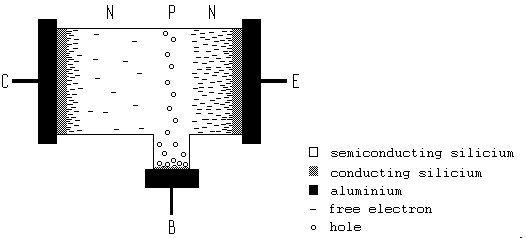
When the transistor is not connected to any voltage source, the base has a voltage difference of -0.7 Volt with collector and emitter. That voltage repels the electrons of the collector towards the collector, the electrons of the emitter towards the emitter, and the holes of the base towards the inside of the base.
Those 0.7 Volt are the energy of the fastest electrons of the collector or emitter: when at random one of them speeds towards the base, it is repelled by that electric field of 0.7 Volt inside the empty zone. It's speed decreases gradually and it stops just when it was going to enter the zone where the holes are. Then, again because of the field, it turns back and accelerates back towards the collector or emitter. Should the field intensity decrease, electrons would be able to enter the zone containing holes. They would recombinate with those holes, and, thus blockaded there, would make that zone become more negative again. That way the electric field increases back to 0.7 Volt. Other electrons will then again be repelled.
Maybe you wonder why you do not measure 0.7 Volt when applying a voltmeter between base wire and emitter wire. The answer is very simple. Whenever two conducting objects made out of different matters touch each other there will allways appear a voltage difference between the two. That's because the piece containing naturally faster electrons will enforce those electrons to the other piece, making it become more negative. This happens also between the transistor wires and the semiconducting zones. Yet if, for example, the voltage difference between the p zone and the base wire is of 4 Volt, then the voltage difference between the n zone and the emitter wire will be of 3.3 Volt. That makes the voltage between the two wires will be of 0 Volt. Whatever combination of different metals you may try to use, you will get the same result: the voltmeter will measure 0 Volt. (Unless one part of the circuit is heat up or cooled down at a place where different conducting matters touch.)
One could think a voltage of 0.01 V would be sufficient for the fastest electrons. That's right, but such fast electrons are very scarce. It is only from 0.5 V on that a minimum of flow is attained. Only some transistors or diodes do show a clear current for base-emitter voltages lower than 0.5 V, down to 0 V.
During the crossing of the no-man's-land, undergoing the electric field of 9 V, the electrons receive each an energy of 9 eV they will evacuate under the form of heat. Inside a transistor, the collector is thus the part that heats up most.
The purpose of the emitter-base current is thus to start the emitter-collector current flow, then to compensate the loss of electrons inside the base. Should the emitter-base battery not compensate those losses, then the emitter-collector current will decrease each time an electron recombinates/disapears. Down to zero. This makes it can take a while before the collector current stops whenever the base battery is removed. That phenomenon can easily be seen on an oscilloscope. If you want the collector current stop immediately, then a negative voltage must be put on the base, in order to repell the electrons out of the base.
Why is the collector thick? Because that way when an important voltage is put between collector and emitter, say 50 V, the electrons of the collector will be able to redraw on a long distance, creating a wide empty zone that will not be crossed by an electric spark that would ruin the functioning of the transistor or even destroy it.
2. Some details about the manufacture
The contacts between the n+, p and n semiconducting zones have not to be made, because they've always existed. One could think the N, P and N zones of a transistor are separate blocks that are pushed against each other. That's not the case: a transistor is a sole monocrystalic block of silicium wherein different zones are created by putting different sorts of ions. Somehow like a Belgian flag made out of one sole piece of cloth, one third being painted in black, the second third in yellow and the third third in red. The color is very important, it is what makes the flag be a flag, yet physically it is only a few miligrams of pigments on a continuous single rectangle of tissue. There is one piece of tissue, not three. (One reason therefore is that if three pieces of crystal where pushed against each other, the two contact zones between them would not be a continuous crystal. Those ruptures into the crystalic continuity would create a lot of unwanted holes and electrons that would disturb everything.)
The reason why the emitter is a n+ semiconductor is the following one:
If an aluminium wire is pushed directly against the p semiconductor of the base, and the whole is heat up, aluminium atoms will penetrate into that p semiconductor and create a very strong local positive doping, p+. Should one try to inject electrons inside the p semiconductor trough the aluminium contact, that will fail: because the electrons must first pass trough that heavily p+ doped zone, full of holes, where they will unavoidably be trapped by recombination with those holes. (Instead of injecting electrons into the base, it will be the base that will deliver holes to the heavily doped contact zone.)
The aluminium / p zone is thus an unavoidable electron trap. The current will go trough without any problem, but it will not be made out of electrons: it will be made out of holes travelling in the opposite direction.
Therefore one solders the aluminium wire on a n+ semiconductor located just near the p semiconductor. That n+ semiconductor will have no problems to allow electrons go into the p zone.
Yet there remains a problem: if when one solders an aluminium contact on a n semiconductor it makes that semiconductor become locally p-doped very heavily, how can we avoid that it erases the local n doping and creates a parasitic diode that will disallow any electron movement? Answer: before approaching the aluminium contact, one dopes heavily, negatively, the surface of the semiconductor, in order it ceases to be semiconducting. It is so full of n ions that it becomes simply a conducting material, just like metal. Thereafter there can no more be erasing by p aluminium ions, because the surface is now a conductor and no more a semiconductor. The added p ions simply make the zone even more conducting.
The electrons passing from emitter wire towards the base will thus cross successively: